May be some resistor deviders in TIA offset need to be recalculated.
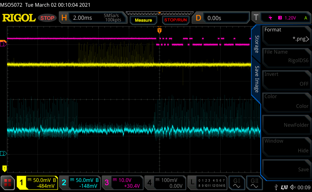
This noise I think from 200 ksps adc in stm.
Yellow is signal after TIA, blue - from second amplifier.
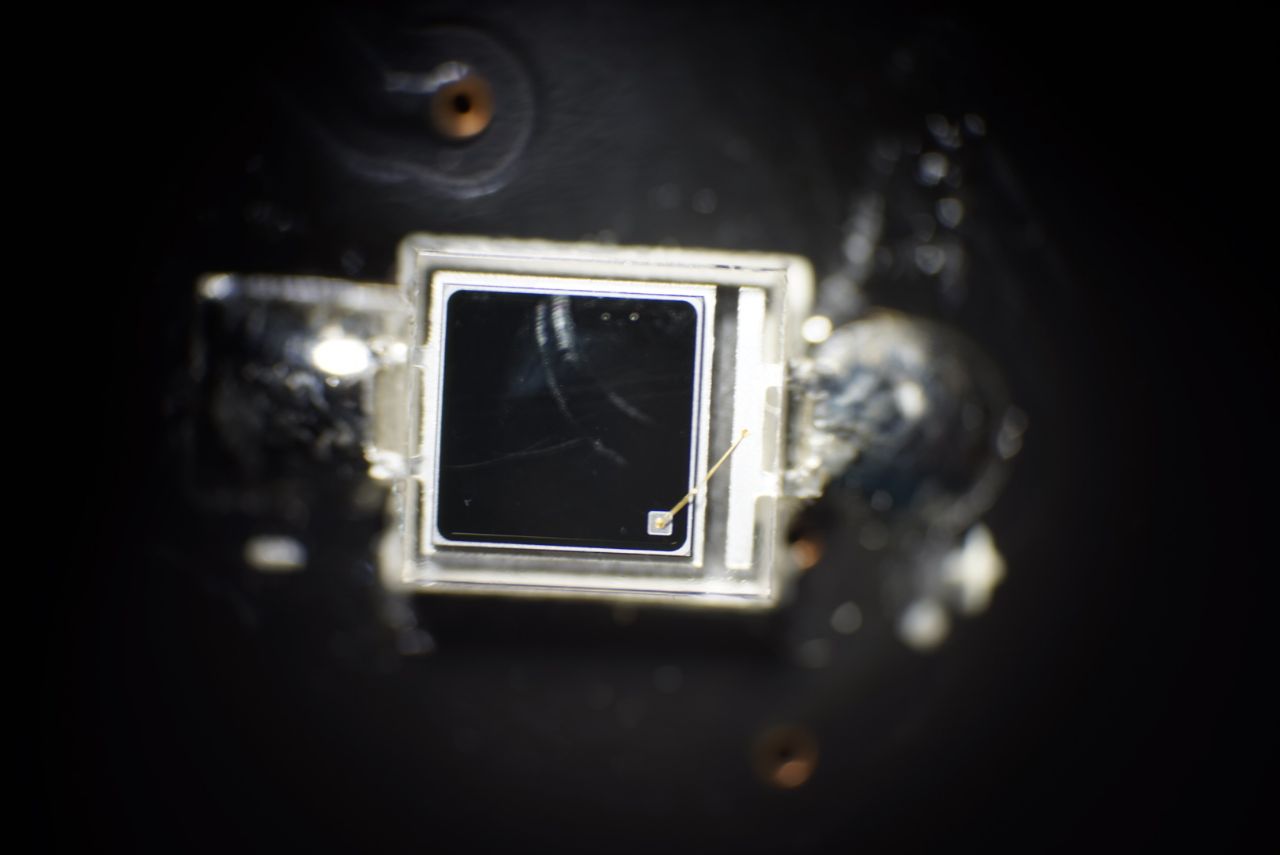
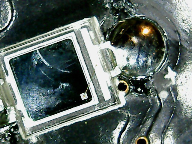
Do we have any part number for photo diode (marked as R4)?
It has 4.5 x 4mm (~4.4 x 3.9mm). From bottom on package I’ve got 7C 23 in two rows in circle.
Looks like Vishay VBP104S but bottom side of diode is a bit different.
Some different contact pad.
I think may be osram sfh2440?
Any ideas how to find exactly the same photo diode? Or should I start buying samples and check them under microscope and make test rig. I’ve got 100MHz oscilloscope, so in theory I could try to characterize them.
I don’t think you can measure any parameter with only oscilloscope.
I think most important parameter is capacitance and response speed.
I should be able to measure response speed using oscilloscope. Or at least compare measured response time between two photo diodes.
1 Like
What type of test rig you want to use?
Basically I was thinking of light source (LED) with matched wavelength to red laser used in SDS011. LED would be driven via function generator. Voltage signal from LED would be on first channel, output from photo diode (via TIA) on the second. I could measure delay from switching on LED to registering impulse from TIA. Just a time difference between two triggers on rising edge. Testing in the same way a different photo diode should result in different average reaction time.
Am I totally wrong? 
You are definitely right.
But there are typical question, which came first, chicken or the egg?
You must have very fast led for it and fast driver, but I don’t know how to measure it without fast photosensor))
Second, there are two common type of photodiodes, with full spectrum (max 800-900 nm) and visual light (max ~600) which one we have?
And third, how wavelength affect on sensitivity of particles different size?
p.s. I noticed that light of flashlight penetrates through “via” holes (even with closed inlet hole) and create big spikes on signal.
And one correction, I think we should consider not difference between rising edges, but width of response. Because with low-pass filtering in tia and capacitance in sensor we will see some smooth signals with slow falling edge.
Science has an answer for that qestion. Egg. Eggs were present long before birds.
The point of making rig is not to fully characterize each photodiode but to compare known photodiodes with unknown diode from SDS011.
Width of response seems to be logical in this situation. Fortunately we can measure both parameters and analyse them later ![]()
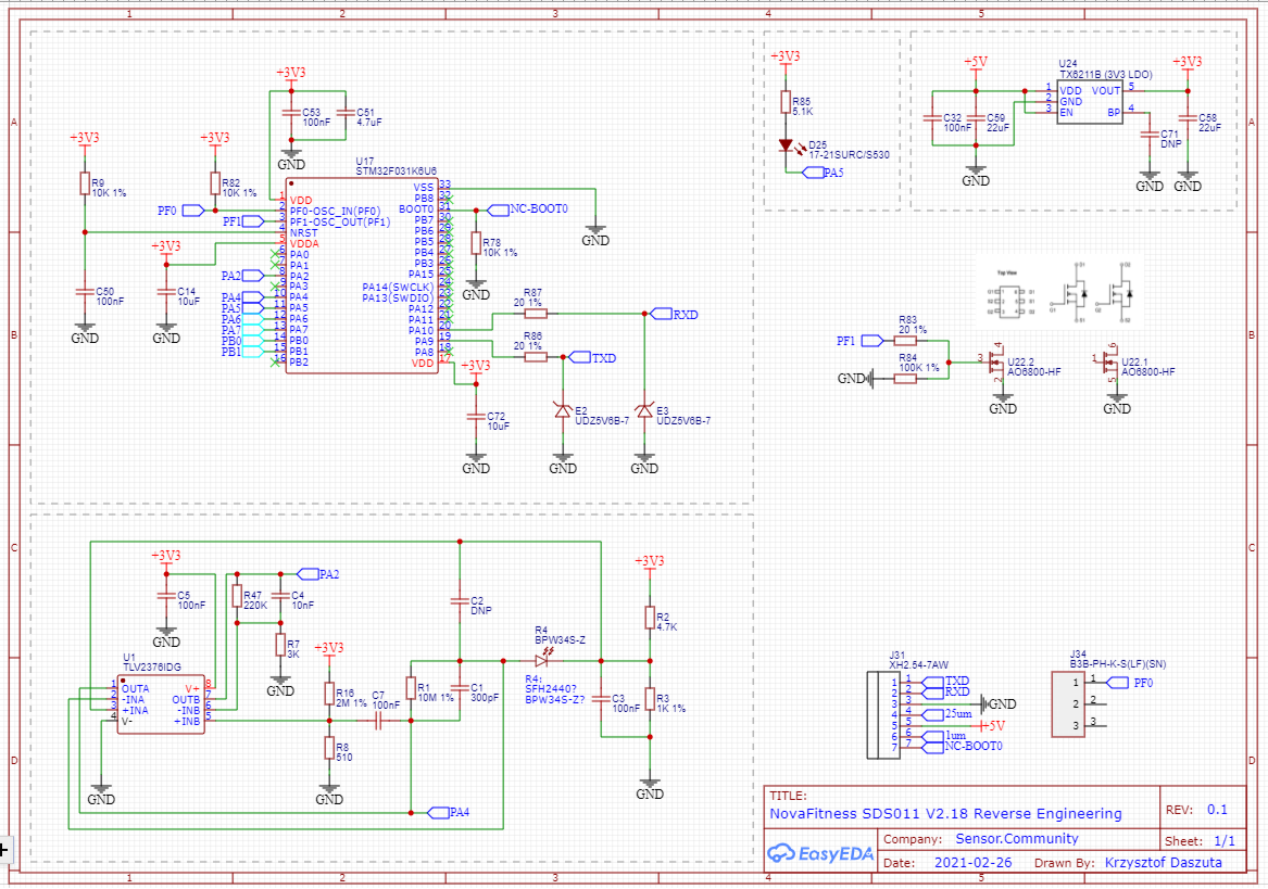
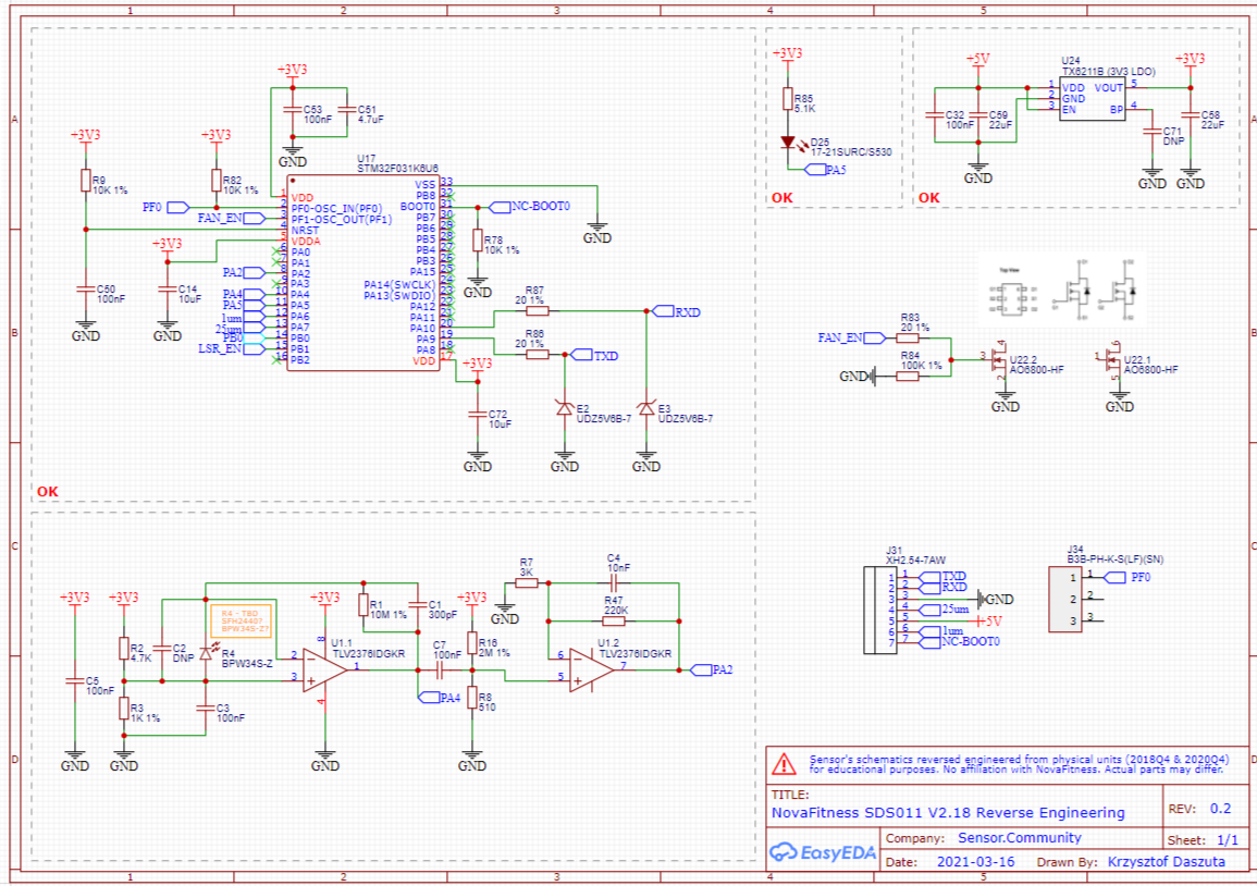
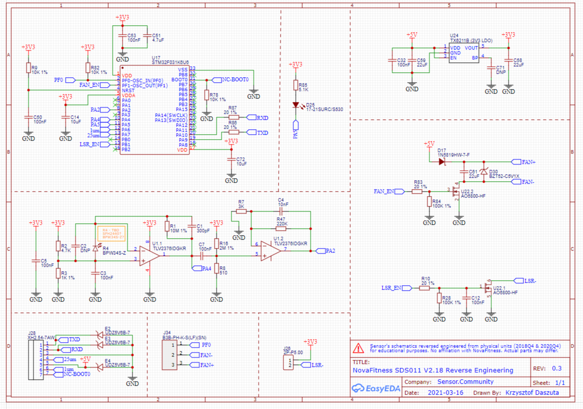
Work in progress. Sections in dashed rectangles are more less finished. @Mogwaika I would appreciate if you could look at TIA section and check if it looks ok.
I would upload PDF, but it is disabled on forums… @Lukas I send you PM couple days ago.
But you should be sure, that led with driver faster, than fastest photodiode.
This looks similar with original sds schematics, but check my scheme in EasyEda that I have shared with you.
There are some common styles of drawing feedback of amplifiers for more clarity.
p.s. I think polarity of photodiode is incorrect.
Yes, I am aware of that. I will try to make it more clear. I need to swap symbol for TLV2376IDG.
Yes! I looked at footprint line mark instead of + and - signs. Thanks ![]()
Oh! That’s nice reference. Especially for TIA section. Thank you.

I desoldered C1 from sds and my multimeter shows ~50 pF. It seems small but I’ll try to check in simulator, is it enough to avoid resonance or not.
What model of multimeter do you use?
uni-t ut71b.
Resolution is 1 pF (Accuracy 1.5 % of value, +/- 20 pF, + capacitance of probes).